On FPGA VI
Hello!
It's running the FPGA VI.
I would just ask you what is the likely cause of the FPGA VI out of different answers every time that I run it (as I'm not closing the VI or change anything in the FPGA VI, I just "re-run").
Thank you!
Hello!
I already solved the problem. I used an other VI to reset (call the method).
Thank you.
Tags: NI Software
Similar Questions
-
Possible to use the main clock FPGA as a basic Source of time for the NI 9234?
Hello
I am running a NI 9234, and NI 9222 module on a cRIO-9114 chassis with a real-time 9022 controller, data acquisition on the 8 channels on the full sample rate, using the FPGA.
My problem is the synchronization of the data, where the NI9234 is usually a late acquisition, compared to the NI9222. I tried manually delay the NI9222 to take the first samples, but so far without success.
To solve this problem and also to ensure a rate of data more comparable on both cards, I was wondering is it possible to create a Source of time Base master for the NI9234 WITH THE FPGA (opposite to import from another NI9234 or similar module)? The NI9222 I already provide with sampling of the impulses from the FPGA (as expected with this module).
Another issue would be the characteristics of the exact chronology of the two modules, including in terms of synchronization between the beginning of the acquisition and the first samples of data. I couldn't find any information about it...
Thank you in advance,
O Hoppe
Hello!
I've never heard of a possibility to use a time base FPGA with a module of Delta-Sigma.
But I think that the question should be what has not worked to delay the signal and how you did it. Have you read this article?
How can I compensate for delays of different group with the C Series Modules in LabVIEW FPGA?
http://digital.NI.com/public.nsf/allkb/74EB238E1BCADD528625735300681A7DCan you give a more detailed description of your trial to delay acquisitions? Can you provide a code example?
Best regards
Christoph
-
LabVIEW FPGA SPI accident - SPI OR IP address for example - R series OR
Hello
I am trying to run the series R - sample project NI SPI FPGA Simulation.lvproj that comes with the SPI IP OR on a real FlexRIO FPGA SMU-7976R target with an attached digital adaptation NI 6581 B Module. The example is for a PCIe-7841R but I wore during my target FPGA, follow these steps and made additional changes to try to make it work with my set-up. I learned that FlexRIO FAMs CLIPs do not work with nodes in office had so I know I can't simulate the project originally planned so I will try to use FPGA to e/s node host side (open FPGA vi reference) to implement the actual hardware.
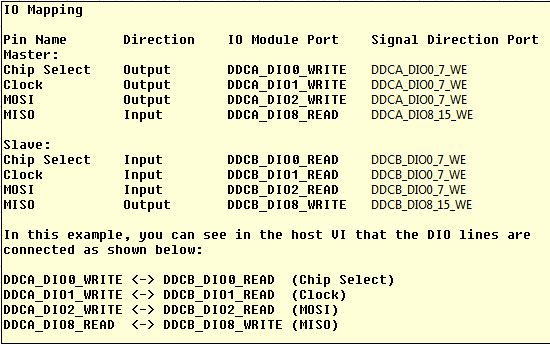
My first question concerns my configuration of the adapter module e/s and selection. I added the IO Module (NI 6581 B: NI 6581 B channel) for my project and selected the channels as shown in the table below. I have a real physical hardware connection as described below using two NI SHC68-C68-D4 cables and a break-out Board.
I changed the names as well:
I selected these DIO channels because I wanted the DDCA connector to be the master and the DDCB connector to be the slave. In addition, in this CLIP every eight channels of i/o has a write enable signal. I have not used the Port configuration because I needed 4 available DIO channels and I saw DIO0-3. Is my logic of selection of channel vs correct Port here?
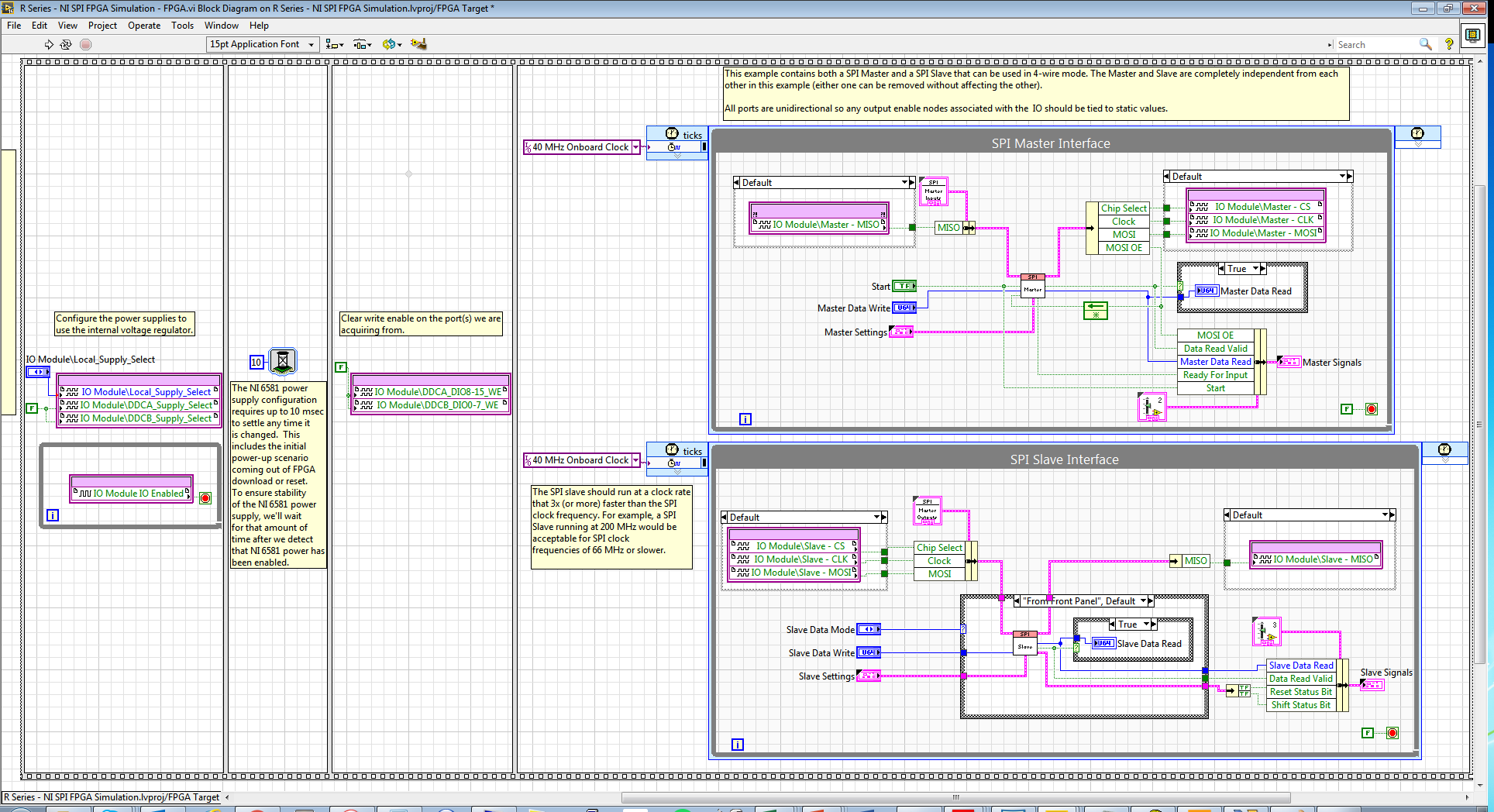
Following the same strategy that examples FlexRIO/NI6581B, I changed the FPGA.vi to include initialization outside of timed loops:
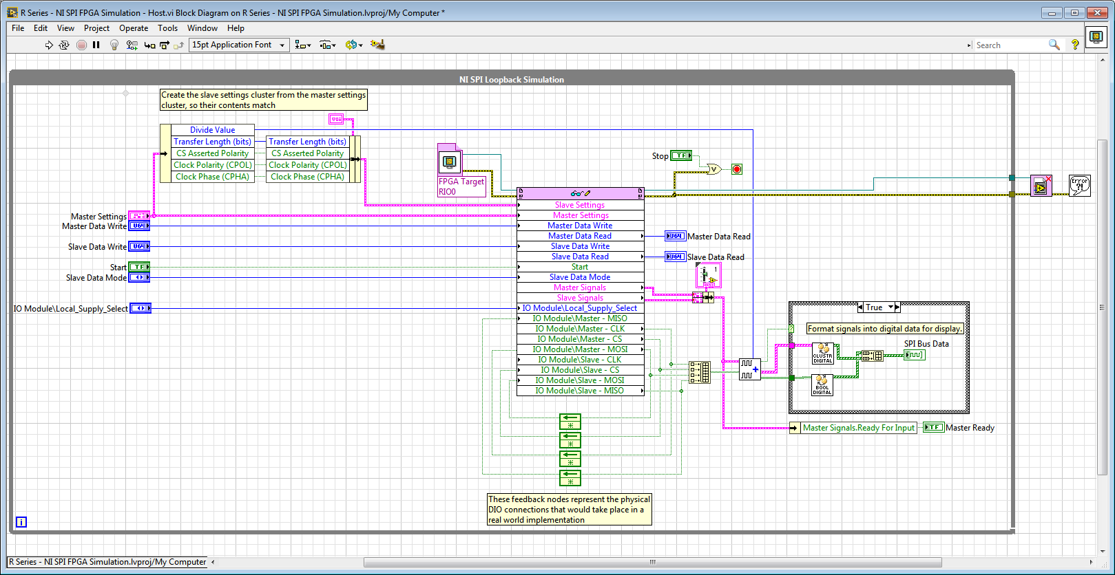
And in the Host.vi I have a node reference FPGA and wired loops of feedback accordingly:
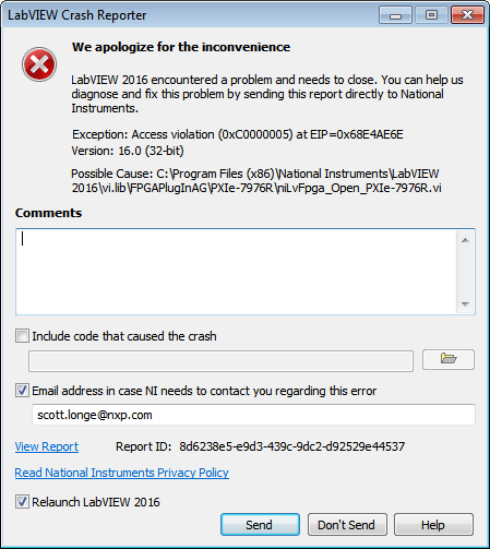
When I compile the FPGA and try to run Host.vi LabVIEW inevitably crashes with Crash Reporter below and must restart:
Does anyone know what I'm doing wrong here? My guess is that it has something to do with the CLIP/IOModule. Any help is appreciated.
Thank you
Scott
Hi Scott,.
I suspect that the problem might be related to the fact that your node open FPGA VI reference is in the while loop and trying to open a new FPGA reference at each iteration.
If you move outside of the while loop, it does not solve the crash?On channel vs port question, your logic seems reasonable to me, but I recommend to try it since this feature could depend on device.
-
I'm looking at the SMU 7857R. I would use the 8 analog inputs and the FPGA to do some annalysisy and DIO based on the best data. I was wondering if it is possible to also define a DAQ task so that all analog data will be made available to the host. Using a data acquisition task would be easier for me to have to write code fpga for use a DMA fifo to send back data.
Hi bcat!
A data acquisition task is only for devices Data Acquisition product supported by driver DAQmx as X-, M-, S-, maps E-Series. The boards of the R series are only supported by the driver OR RIO.
If you don't need pre-treatment on the FPGA so that you can distribute simple data through DMA on your host. If you are looking for an API for the comparable FPGA with the DAQmx API then please check the NI CompactRIO waveform reference library. You can also use the library for R Series boards. -
FPGA/FPGA adapter creates 250 mV voltage offset
I use a high-7971R FPGA in a chassis SMU-1073 with the adaptation Module 5782 (DC coupling) and 2016,08 device drivers. When I turn on the chassis and my computer, nothing strange happens. When I try to run something on the FPGA, however, things get weird. Each piece of code works exactly as it should, but as soon as that 'open FPGA reference' finishes running the adapter begins to produce a voltage mV to 0 to + 250 Ai and AI 1. It doesn't go to AO 0 or 1 AO. This shift of power disappears temporarily as long as 'Reference FPGA open' or "Close FPGA reference" are running, but the only way to get rid of the tension of offset entirely is to restart the chassis. Can someone explain to me why this is happening and how to fix it? The FPGA code, I am running can handle a small shift, but this shift seems to be to saturate the signal.
To see the shift: branch I HAVE 0 and AI 1 directly in a 1 M complete oscilloscope.
It is planned. CDA on this FAM (and more high-end a/d converters) have a range of sampling which is not centered around zero. The front end of the compenstates of the FAM for this by applying an offset from the signal which would appear to the user that the range of the ADC is centered around zero. What is different between this FAMILY and other instruments, is that it is not an additional circuit preventing that this lag observed a user of height of the output of the analog input.
You see the shift happen to reference open FPGA is because that's when power to the GPA is activated. The shift should not have an effect on reading which provides the analog input. Just make sure you have impedance corresponding to the source of the signal at the analogue input and you should be good.
-
Band bandwidth SMU for FPGA chassis
I'm specing on material for an FPGA FlexRIO system. The module FPGA and adapter, we will use has already been defined, a 7975R and a 5782. For our application, we will be streaming 2 inputs analog on a RT controller attached. From my understanding, these samples will be single precision floating point numbers, each of which is a piece of 4 bytes. Assuming that the 5782 max sampling rate is used, 250 MECH. / s, I think that I will need 2 GB/s of bandwidth on my SMU chassis.
Here my question, then, what SMU chassis should I consider? The SMU-1082 has "up to 2 GB/s per-slot dedicated bandwidth", but it is a real or theoretical number? Normally, I would just get the next thing that high, just to be sure, but there is a significant price difference on the way to the SMU 1085, which is also much larger I need. So I would like to save space and several thousands of dollars if I could get away with a 1082. Sampling does not quite to the max modules of adaptation would be acceptable, but I would be interested to know where about my maximum sampling speed would be.
Thanks in advance for your help.
The 1082 has more than enough bandwidth to stream data at a time to the analog inputs of a 5782. The 5782 has a 14 bit ADC with two channels that sample to 250 ms/s. These samples are returned as an I16 with the two least significant bits filled with zeros.
So assuming that you transfer all I16, rather than packing the 14 bits of data, you would have the following bandwidth requirements.
2 channels x 2 bytes/sample x 250 mega-samples per second = 1 GB/s
The 1082 a 2 GB/s of throughput dedicated per slot. The 7975 accommodates up to 1.6 Gbps streaming. I would recommend calling chat with someone, if you are looking for a recommendation on what type of chassis to purchase, but based on the requirements of streaming that you're fine with the combo 7975 and 1082, you thought. Just make sure you get a controller which can accommodate streaming speeds you're looking for. The 8840 is a good candidate.
-
Hello
I would like to smooth out motion of my linear motor. For example, I would like to start a program on the cRIO in scan mode Let's say 1ms interval scan and then perform the interpolation between the points of output (for example, the wave of fishing) on the scan interval 100us. FPGA I wrote programs little but my linear motor does not move. I can't find where I made a mistake or / and something is missing.
Any help would be approciated.
I put in the attachment of my FPGA file, but also the host file I have on the cRIO.
Thank you.
Kamil
Dear Alex,
Thank you interested in my topic. I just understood how do. I went by this example: http://www.ni.com/product-documentation/3598/en/. However I have modyfied somewhat FPGA interpolation method. One described is nove myself smooth enough movement. I have attached files if anyone will need one day. I think that the case is closed.
-
Hello
I use card FPGA 7966R with Module of e/s 6587. I have two sets of screws FPGA, one that uses 6587 mode series (Serdi channel) and the other in parallel mode (Serdi connector). I'm trying to select one of the FPGA VIs via the host VI and I don't know if it's possible.
Some things to note:
- All IOs have the same names, FIFO has the same data type and name.
- Because they use the IO 6587 controller in a different configuration, I can't parallelize them and combine them into a single VI.
Thank you
MILIN
You should take a look at the function of Bitfile dynamic reference opened .
-
Control of read/write of FPGA Interface
I need help on control of FPGA read/write Interface. I would like to connect data TCP Read (String) directly to VI FPGA Read, but the entrance is an FXP... How can I do this?
Then change your FPGA control to be a byte (U8). On the side of your host, use the array of strings of bytes, then Index Array to get the specific byte you want to write on the FPGA.
-
Digital electronics FPGA Board Hardware Driver for Windows 10
My son just made me aware that his school has a dozen of National Instruments Digital Electronics FPGA boards, but they have never been able to get them to work or actually use them in the curriculum. It seems that he has left his instructor know that I worked with FPGA Xilinx for more than 10 years and now everyone counting on me to get these maps work. The issue seems to be the USB driver. According to the manual, I tried DEFB2012_5_2.exe which simply refused to run on this machine Win 10 x 64. DEFB_4_3.exe ran, but complained that LabView components have not been installed and that it would not continue. Could someone tell me please how to install USB driver ONLY so that we can download files of bits with IMPACT? In terms of a school budget, the investment they have in these maps is not negligible. Thank you.
Hello Dave and TGregor,
I hope I can clear some things here. I'm sorry that you run in so many questions with your boards OF FPGA.
First of all, direct responses:
The LabVIEW FPGA 2015 driver should install the components needed to use the Board with Xilinx tools on WINDOWS 7, it will not work on any system more recent that the pilot has been developed before the release of Windows 8 and 10.
http://www.NI.com/download/NI-Digital-Electronics-FPGA-Board-driver-software-2015/5857/en/
My recommendation for Windows 8 or 10 is rather install Xilinx ISE you find on Xilinx website or on the downloads page OR:
https://www.Xilinx.com/products/design-tools/ISE-design-suite.html
http://www.NI.com/download/LabVIEW-FPGA-Module-2016/6231/en/
The difficulty that you face here is that tool Xilinx ISE is officially supported only on Windows 7 and below. So even though I think it will work (and it will move to the difference in the link of the above driver OF FPGA) for Windows 8 and 10, you can continue to deal with certain issues.
Now you are all looking to program the FPGA using an HDL, Multisim and LabVIEW? If you just use an HDL, you should be all set to go and in the dev environment, you had planned using the program. Circuit design of Multisim 'S simulation tool which includes a complete library of graphic digital components. A digital circuit can be built using the graphical logic gates in Multisim then downloaded directly on the FPGA without first having to learn VHDL or Verilog. It is quite popular among the logical classes digital introduction and we can help you by establishes that as well if you are interested.
For anyone else who might stumble upon this page, I want to make sure you are all aware that, while the Board of Directors OF FPGA is still supported and sold, it has been developed a number of years and has recently been replaced by the Council for development of the digital system (DSDB)that uses a 7020 architecting and has much periphrials more to the program than the FPGA OF. So I know that it is not useful for the current issue, but anyone looking for if they would like to buy more OF FPGA boards, I recommend watching the DSDB instead.
Thank you!
-
Hi all
Please, for the love of God can someone take a look at the attached FPGA project, I hit to the top and tell my why it is that whenever I run, as soon as he's trying to read/write on the host computer, it returns error-61046? A screenshot of the error is included in the attached .zip file.
I made many programs FPGA before with no problems, while using the same FPGA and FlexRIO module and never had this problem. If I run an example program it works fine so I am confident, that the error lies in my programming, I can just see where!
As you can see all the clocks are internal and appear to be configured correctly according to the example programs and other programs FPGA, that I have done before, so I'm puzzled. I hope that it is just my stupidity and lack of coffee.
Congratulations in advance.
Mitch
The pilot FlexRIO comes two CLIPs for the 5781. At ' a "NI 5781 Sychronous system" OR 5781 "VIDEO CLIP.
The "NEITHER 5781' is what originally delivered with the FAM and is always delivered with the driver for legacy purposes. I would discourage the use of this CLIP because it uses regional clocks for IO Module clock 0/1 which limit the amount of fabric that can be driven by these clocks to the fabric available in the respective region of the FPGA. The advantage of this CLIP, it's that the ADC and DAC can be clocked at different rates through a clock divider that exposes the CLIP.
The 'NI 5781 Sychronous system"CLIP is what is recommended for all new models. It uses a world clock which can target tissue in all regions of the FPGA. This CLIP uses the same clock to drive the ADC and DAC (IO Module clock 0). IO Module clock 1 is not used in this CLIP.
If you used the sychronous CLIP system and always a logic had driven out by IO Module clock 1 it that would explain why you received the error of non-response from IO Module clock 1 is left connected in the sychornous CLIP system.
-
Reverse and pseudo inverse Matrix on FPGA
Hi all
How can I calculate matrix inverse/pinv on pushed more logical clock (*.gcdl), for FPGA? (Labview Comms 2.0)
Maybe someone has a solution for this task? Or that the best algorithm I use for this task?Thank you.
Hello togoto,.
We have matrix Inverse and matrix screw Pseudo-inverse for code side host, but these are not supported on FPGA. The reason for this is because without a known matrix size, there is not a way to implement a dynamic matrix math function (the compiler couldn't know how many resources which requires). If we consider that more algorithms of inverse depend on the division, which is very intensive on FPGA resources, which provides another reason why we would be unable to put implementation in CDL.
That being said, Comms has Matrix multiply and transpose the matrix of features that you can implement in CDL. Because for a long time the matrices are always a fixed size and uniform, you can implement a custom algorithm to achieve pseudoinversion and matrix inversion. It would take careful pipelining to ensure it worked in a single clock cycle.
Could you elaborate on what exactly the application is supposed to accomplish? If possible, the math movement matrix your screw host-side may be the best approach.
Best,
Daniel
-
Hello
I can generate a C API interface for FPGA design in Labview Communications.
And how does it work?
Thank you
Sebastian
Hi Sebastian,.
If it is anywhere in the LabVIEW Communications, he'll be in tools Launcher. If it is not there then you can still generate a C API for your FPGA using the FPGA Interface C API generator. I received this the generating a C API for a help Application LabVIEW FPGA Document.
Generating a C API in the Windows Start Menu
Follow these steps to generate a C API for a bitfile compiled in the Windows Start menu.
- "" "" Select Start "all programs" National Instruments "FPGA Interface C API" FPGA Interface C API generator.
- On the Generator of API C FPGA Interface dialog box that appears, navigate to the compiled FPGA bitfile or type an absolute path for her.
- Select a directory for output to the C API. If you do not select an output directory, the files in the C API will be created in the directory that contains the bitfile. You can navigate to a directory or type an absolute path for her.
- Optionally, you can change the prefix for the generated files and constants in the generated .h file.
- If you are using LabWindows/CVI to develop your C application, check next to exclude NiFpga.h/NiFpga.cas FPGA Interface C API installs the header and library files with the support of LabWindows/CVI.
Make sure you have installed FPGA C Interface API .
Introduction to the API of C Interface of FPGA
See you soon
-
Mode of scanning/FPGA for a CRIO by Veristand
Hello!
I have a small error using my CRIO 9081 use with CAN communication, here's what I did:
1. I use the CRIO with scan mode and customized it "Scan engine" and Ethercat for show my analog modules under VeriStand, it's ok
2. I use the CRIO with FPGA Scan interface (together under Labview) to detect my modules CAN, also ok
3 - then I wanted to see the CAN and analog modules, so I use this page:
http://digital.NI.com/public.nsf/allkb/0DB7FEF37C26AF85862575C400531690
And here's my problem:
with this method I am able to see the two modules with the custom device 'analytical engine and ethercat", which is really nice, BUT, impossible project VeriStand, the error message asking me to turn the chassis using FPGA, but then I lost the analog module...
So is it possible to run a project Veristand using both Scan and FPGA interface mode?
Thank you very much

Hi Vincent,.
When you tried to implement, you use the procedure described in the following document in the section use of Scan Engine and EtherCAT with NI 986 x custom device modules XNET ?
From what I remember, because you use a cRIO-9081, you will need to compile an empty bitfile for your target and place the controller in Mode FPGA hybrid mode on your chassis.
Could you post a screenshot of the error of deployment, you see?
-
How to read the status of User1 DIP-switch with a cRIO FPGA chassis?
How to read the State of the DIP switches on a FPGA cRio chassis?
I work with a cRIO 9022... My idea is to put the system in "service" mode with USER1 switch to IT and communicate with the FPGA via the FPGA - GUI (VI) on the host computer instead via the RT module that is used in normal conditions.
Any ideas? Unfortunately, I don't have an unused channel on the left... .and (as I know) cannot use the interface RS232 of FPGA.
Many thanks in advance,
Luke
Hi, this is the correct information. You cannot read the FPGA of DIP-switch status. The only thing you could do is to use the function of Reading Switch.vi located under the range of functions-> real-> utilities RT time
It's how you probably know side host RT and not the FPGA.
Cordially Virginia
-
SMU-7975R with FPGA Kintex-7 - LVDS problem
Hello
I developed a custom RIO FLEX module (Digitizer18, 0xAB66 - vendor id) and try to use it with the card 7975R-SMU-FPGAS (FPGA Kintex-7)
I have a problem, try output LVDS signal via aUserGpio (61) and aUserGpio_n (61).
These pins are not K7 capable clock, but I used this module FLEX RIO with SMU-7962R (Virtex-5 FPGA) where these pins are capable REGIONAL clock and it worked fine.
Kintex-7 it compiles without error, but I see no signals on the pins aUserGpio (61) and aUserGpio_n (61), although its switching State is ADC2_FSM.
Is it possible to use pins that is not capable of WHAT LVDS output or I am condemned to use MRCC clock or pins SRCC?
Thank you
My xdc file (aUserGpio (61) and aUserGpio_n (61) belong to the 18 Bank):
set_property IOSTANDARD LVDS_25 [get_ports {aUserGpio [61]}]
set_property FAKE DIFF_TERM [get_ports {aUserGpio [61]}]
set_property IOSTANDARD LVDS_25 [get_ports {aUserGpio_n [61]}]
set_property FAKE DIFF_TERM [get_ports {aUserGpio_n [61]}]# all unused pins Bank 18 are LVCMOS25
set_property IOSTANDARD LVCMOS25 [get_ports {aUserGpio [49]}]
set_property BUNCH SLOW [get_ports {aUserGpio [49]}]
set_property DRIVE 8 [get_ports {aUserGpio [49]}]
set_property BIO FAKE [get_ports {aUserGpio [49]}]...
part of my clip to vhd file (because it's too big and all other LVTTL logic works very well except LVDS):
attribute dont_touch: string;
Signal ADC2_CNV_buf: std_logic_vector: = '1';
attribute dont_touch of the ADC2_CNV_buf: signal is 'true '.OBUFDS_ADC2_CNV: OBUFDS
map of port)
O-Online aUserGpio (61)-Diff_p output (connect directly to the port of higher level)
OB-online aUserGpio_n (61)-Diff_n output (connect directly to the port of higher level)
I have-online ADC2_CNV_buf - the input stream
);....
process (LVDS_CLK) - 200 MHz
Start
If LVDS_CLK' event and LVDS_CLK = "1" then
ADC2_FSM case is
When s0 =>
If ADC2_CNV = "0" then
ADC2_timer1 <= (others="">' 0');
ADC2_timer2 <= (others="">' 0');
ADC2_CLK<=>
ADC2_READY<=>
ADC2_CNV_buf<= '1'="">
ADC2_FSM<=>
end if;
When s1 =>
If ADC2_CNV = "1" then
ADC2_CNV_buf<= '0'="" ; ="" ="" ="" ="" ="" ="" ="">
ADC2_RESET<= '1'; ="" ="" ="" ="" ="" ="" ="" ="" ="">
ADC2_FSM<=>
end if;
When s2 => ADC2_FSM<=>
When s3 => ADC2_FSM<=>
When s4 => ADC2_FSM<=>
When-online s5
ADC2_CNV_buf<= '1'="" ; ="">
ADC2_RESET<=>
ADC2_FSM<= s6;="" ="">
When-online s6
If ADC2_timer1< x"28"="" then="" --="">
ADC2_timer1<= adc2_timer1="" +="" 1;="">
on the other
ADC2_FSM<=>
end if;
When s7 =>
ADC2_CLK<= not="">
If ADC2_timer2< x"24"="">
ADC2_timer2<= adc2_timer2="" +="">
on the other
ADC2_READY<=>
ADC2_FSM<= s0; ="" ="">
end if;
When other => ADC2_FSM<= s0; ="">
end case;
end if;
complete the process;-the host uses the flank amount of DCO± to capture D±
process (UserGClk2, ADC1_RESET) - echo DCO2 clock
Start
If ADC1_RESET = "1" then
ADC2_READ_FSM<= s0; ="">
ADC2_BUF <= (others="">' 0');
elsif UserGClk2' event and UserGClk2 = '0' then - host uses the flank amount of DCO± to capture D±
ADC2_READ_FSM case is
When s0 => ADC2_BUF (17)<= not="" d2="" ;="" adc2_read_fsm=""><=>
When s1 => ADC2_BUF (16)<= not="" d2="" ;="" adc2_read_fsm=""><=>
When s2 => ADC2_BUF (15)<= not="" d2="" ;="" adc2_read_fsm=""><=>
When s3 => ADC2_BUF (14)<= not="" d2="" ;="" adc2_read_fsm=""><=>
When s4 => ADC2_BUF (13)<= not="" d2="" ;="" adc2_read_fsm=""><=>
When s5 => ADC2_BUF (12)<= not="" d2="" ;="" adc2_read_fsm=""><=>
When s6 => ADC2_BUF (11)<= not="" d2="" ;="" adc2_read_fsm=""><=>
When s7 => ADC2_BUF (10)<= not="" d2="" ;="" adc2_read_fsm=""><=>
When s8 => ADC2_BUF (9)<= not="" d2="" ;="" adc2_read_fsm=""><=>
When the s9 => ADC2_BUF (8)<= not="" d2="" ;="" adc2_read_fsm=""><=>
When s10 => ADC2_BUF (7)<= not="" d2="" ;="" adc2_read_fsm=""><=>
When s11 => ADC2_BUF (6)<= not="" d2="" ;="" adc2_read_fsm=""><=>
When s12 => ADC2_BUF (5)<= not="" d2="" ;="" adc2_read_fsm=""><=>
When s13 => ADC2_BUF (4)<= not="" d2="" ;="" adc2_read_fsm=""><=>
When s14 => ADC2_BUF (3)<= not="" d2="" ;="" adc2_read_fsm=""><=>
When s15 => ADC2_BUF (2)<= not="" d2="" ;="" adc2_read_fsm=""><=>
When s16 => ADC2_BUF (1)<= not="" d2="" ;="" adc2_read_fsm=""><=>
When s17 => ADC2_BUF (0)<= not="" d2="" ;="" adc2_read_fsm=""><=>
When s18 => ADC2_READ_FSM<=>
When other => ADC2_READ_FSM<= s0; ="">
end case;
end if;
complete the process;
ADC2_DATA<= "00000000000000"="" &="" adc2_buf="">I've made a few changes to TestCLIP.fam:
...
[FlexRIO-K7IOModule]
DefaultCLIP = TestCLIP
VccoLevel = 2.5...
And my xdc file now looks like this:
# Set the voltage from Bank to Bank 18.
#set_property IOSTANDARD LVCMOS25 [get_ports-filter {IOBANK == 18}]set_property IOSTANDARD LVCMOS25 [get_ports {aUserGpio [*]}]
set_property IOSTANDARD LVCMOS25 [get_ports {aUserGpio_n [*]}]
set_property IOSTANDARD LVDS_25 [get_ports {aUserGpio [58]}]
set_property IOSTANDARD LVDS_25 [get_ports {aUserGpio_n [58]}]
set_property IOSTANDARD LVDS_25 [get_ports {aUserGpio [67]}]
set_property IOSTANDARD LVDS_25 [get_ports {aUserGpio_n [67]}]Now it's working.

Maybe you are looking for
-
IPhoto on external drive said updated
I have then all my family photos (about 300 GB) on an external drive about 2 years ago. Today I tried to open my iphoto on the external hard drive and I got an error message that says "iphoto cannot be opened white it is updated. As far as I know, it
-
Office jet pro 8625: ink cartridge levels
Don't really see instructions on this printer and I wonder if there is a way to determine which cartridge is low on ink when the error message appears. I thought having the distinct colors would allow me to change only what he needed, but I can not s
-
Trying to right click and send to specific folder, it is not available
When I want to send data to a specific to say 'documents' folder I right click, but do not get this option how to do that please?
-
I am trying to download Coupons.com and my computer won't let me. I am using Windows Internet Explorer? Or I would like to recover my toolbars for coupons. But don't know how
-
Import of email in outlook in windows live mail
Hello Recently, I have set up a new computer and started using Windows Live Mail, Windows 7 Home Premium. Since then, I decided to use Outlook 2010 instead of Live Mail. On the Windows Live Mail Export Panel, there are two options, "Microsoft Exchan