Or Digital Electronics FPGA Breadboard UCF
Nice day.. I use Xilinx ISE 14.3 to program my NI Digital Electronics FPGA Board and I want to use some FPGA GPIO lines placed on the area Breadboard1 (BB1)... how I can create my file FCU to use this GPIO. ??
Hello $ T - Rex,.
Thank you very much for your help. I really apprecaite this... that's what I really need...
Thank you very much!
Tags: NI Products
Similar Questions
-
Digital electronics FPGA Board Hardware Driver for Windows 10
My son just made me aware that his school has a dozen of National Instruments Digital Electronics FPGA boards, but they have never been able to get them to work or actually use them in the curriculum. It seems that he has left his instructor know that I worked with FPGA Xilinx for more than 10 years and now everyone counting on me to get these maps work. The issue seems to be the USB driver. According to the manual, I tried DEFB2012_5_2.exe which simply refused to run on this machine Win 10 x 64. DEFB_4_3.exe ran, but complained that LabView components have not been installed and that it would not continue. Could someone tell me please how to install USB driver ONLY so that we can download files of bits with IMPACT? In terms of a school budget, the investment they have in these maps is not negligible. Thank you.
Hello Dave and TGregor,
I hope I can clear some things here. I'm sorry that you run in so many questions with your boards OF FPGA.
First of all, direct responses:
The LabVIEW FPGA 2015 driver should install the components needed to use the Board with Xilinx tools on WINDOWS 7, it will not work on any system more recent that the pilot has been developed before the release of Windows 8 and 10.
http://www.NI.com/download/NI-Digital-Electronics-FPGA-Board-driver-software-2015/5857/en/
My recommendation for Windows 8 or 10 is rather install Xilinx ISE you find on Xilinx website or on the downloads page OR:
https://www.Xilinx.com/products/design-tools/ISE-design-suite.html
http://www.NI.com/download/LabVIEW-FPGA-Module-2016/6231/en/
The difficulty that you face here is that tool Xilinx ISE is officially supported only on Windows 7 and below. So even though I think it will work (and it will move to the difference in the link of the above driver OF FPGA) for Windows 8 and 10, you can continue to deal with certain issues.
Now you are all looking to program the FPGA using an HDL, Multisim and LabVIEW? If you just use an HDL, you should be all set to go and in the dev environment, you had planned using the program. Circuit design of Multisim 'S simulation tool which includes a complete library of graphic digital components. A digital circuit can be built using the graphical logic gates in Multisim then downloaded directly on the FPGA without first having to learn VHDL or Verilog. It is quite popular among the logical classes digital introduction and we can help you by establishes that as well if you are interested.
For anyone else who might stumble upon this page, I want to make sure you are all aware that, while the Board of Directors OF FPGA is still supported and sold, it has been developed a number of years and has recently been replaced by the Council for development of the digital system (DSDB)that uses a 7020 architecting and has much periphrials more to the program than the FPGA OF. So I know that it is not useful for the current issue, but anyone looking for if they would like to buy more OF FPGA boards, I recommend watching the DSDB instead.
Thank you!
-
Playback of digital input [FPGA] - NI 9401 - questions?
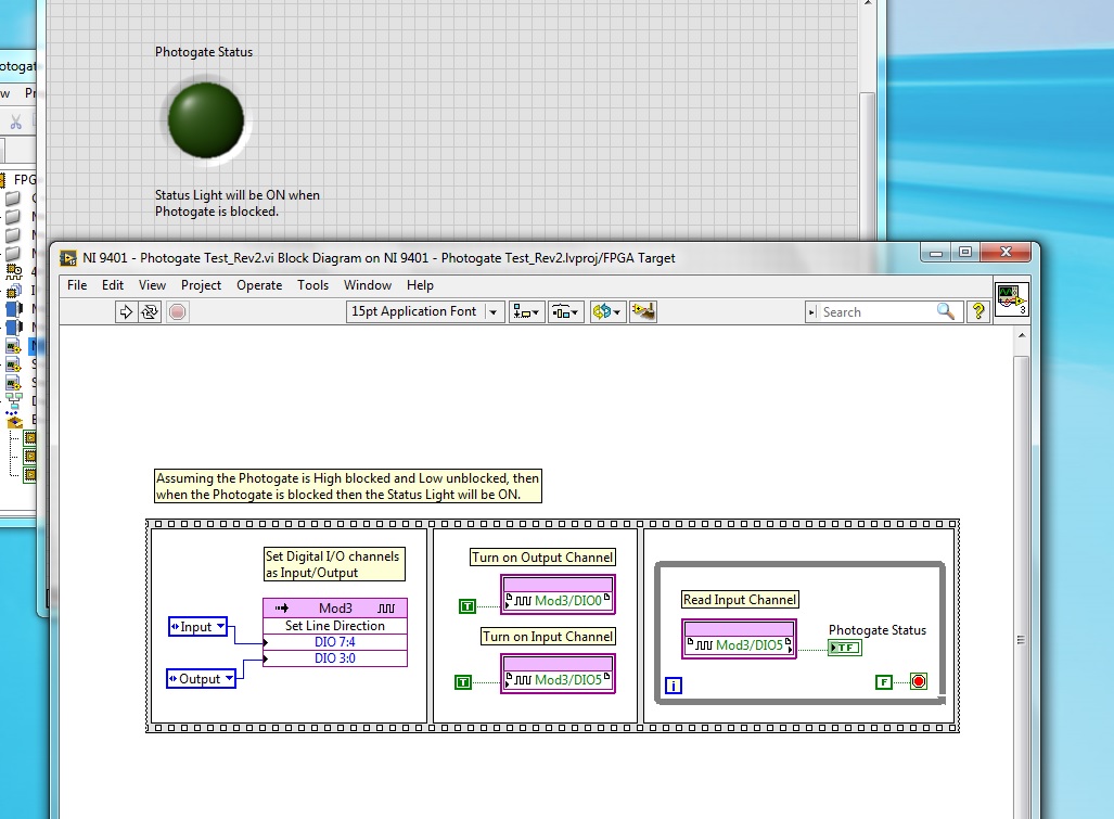
I'm having some trouble with the digital input NI 9401, which is to have a uniform reading. I have a photogate that power of a digital output is turned off and goes in to a digital input module, but I can't read the entry several times. My LED flashes once and never again will blink until I restart my CRIO or recompile. I have launched the ports of entry and exit, their market and constantly for loop. Any idea what's going on?
Hi Allan,
Why you "light up" a channel of entry?
Writing a value to a DIO PIN is usually for outings!
What is connected to your PIN DIO 5? Have you checked the entry with a DMM measure?
How long the impulses are measured with this entry? Do you really you can see short pulses of light flashing?
-
How do I create a traction voltage as a control signal upward?
I use a minimum/maximum statistics module, but is unable to route the analog data to all 16 entries that I need this module (I suppose a limitation of current car, but I don't know why this would be necessary in the software). My first thought was to use a Signal Amplitude controlled router to expand this case 15th signal at 16. It seems that, since I want the router to Signal to be always active (ON) that I don't want to pull up to command input the Signal from the router. How to create a pull upward which is common in digital electronics for this?
It is not a limitation of current car, but simply that you can plug a wire 15 times, for up to 16 destinations. You can work around this by inserting a module of scaling, the NOP value, then its output for up to 16 more destinations.
-
Hi all
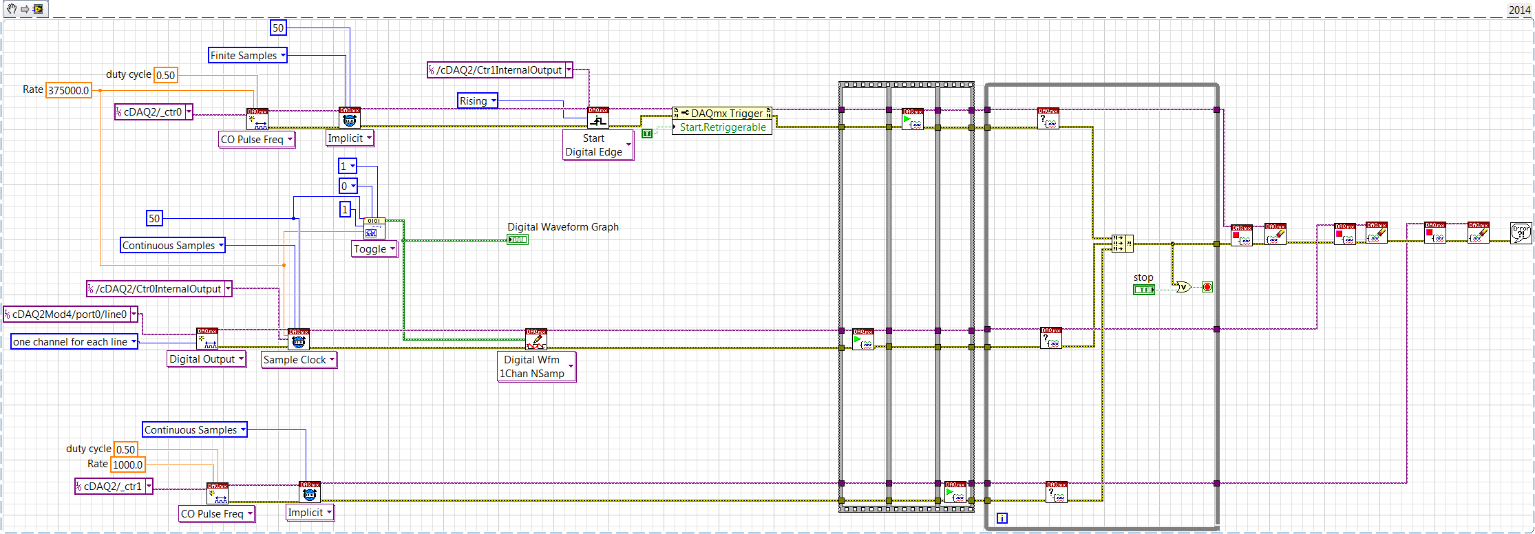
A complex project I have to implement an interface acquisition of material for a linear motion sensor using the output of the synchronous serial (SSI) commune in the control of the industrial movement. (I have a bit of experience in digital electronics, but I'm new to hardware synchronized timer e/s digital in LabVIEW).
To do this, I need to create a clock timed by the busted hardware signal pulse train TTL. Each burst consists of 25 down transitions, with a period of complete cycle of 2.67 microseconds (375kHz). The output is then held high until the next outbreak, that produce at 1ms intervals.
Using of cDAQ timers and a NI 9401 (based on the example http://www.ni.com/example/30256/en/), I was able to create the pulse train burst as described (see attached image VI). Then I need to configure another timer to set off this explosion to repeat at 1ms intervals.
Someone at - it guidance on how best to accomplish the hardware timing for the repetition of the pulse train?
Any suggestions of alternative strategies or observations about the way that my noobish code is stupid or ineffective are welcome as well!
Thank you!
Hello RyanBiggs,
You will need to perform the following operations based on the code that you have joined.
- Set up a second output continuous counter task which will give an impulse to 1000 Hz.
- Set up your first task of meter output to start according to the configuration in the first step using the vi DAQmx trigger.
- Configure the first task of the meter output to redeclenchables via the property node so that the output meter pulses when he sees a rising from the second task of meter output.
The implementation is shown below.
Kind regards
Izzy O.
Product Support Engineer
NI.com/support
-
Mod 10 down back to 8 and does not pass 7
Can someone move this to the forum of Multisim? I can only put in Circuit Design Suite.
In any case, I have problems with Multisim. I made more complex circuits, but somehow, I lost my memory and cannot remember it clearly. So I go on Digital Electronics 1, I'm ready for Digital Electronics 2.
I am a 15 low meter mod. To happen 15 to 0 easily, but I want him to be 9-0, then the display shows 9, 8, 7, 6, 5, 4, 3, 2, 1, 0 and 'LOAD' then 9 and countdown again.
Without the charge, he would go 15 - 0 and reset.
So in class, we learned at 15 (1 1 1 1) NAND to load presets ABCD, I used a switch is customizable. I use 1001 for 9-0, but he is always put back to zero (load) to 7... So there are 9, 8, 9, 8, 9, 8, 9, 8 and so on.
It will count down to 0 and go back to 15, but at 15 he flip 1111 to a low and will activate the load and given to 9. I can't get it past 8. I can move the ABCD to 6, and it works perfectly. It will go from 6 to 0 and then load back to 6 and repeat. When I try from 9 to 0, it just will not work.
Any idea? Someone asked me (since I took the Multisim from Digital Electronics 1 section and he took the model section) if it must use the DIP switches and how the teacher said no cause of bounceback? She also told my partner to use only one... but I don't remember if it was instead of the clock, OR switches. I see people on Multisim using buttons instead of my switch. What is the problem?
In addition, my display 7 segments will not work correctly.
So, my teacher asked me what was the model number for the NAND and I didn't.
She told me to Google the model number and then use in Multisim.
I've done that I have placed a NAND4 - not a 7420N.
I knew that the NAND dirtied with the count of 9-0. So, we replaced by a 7420N and there are now 9-0.
To display, I did it properly and did so my classmates - but the default is 7446 somehow does not work and shows the numbers in front of what he has. So ONE looks like a three backward, because it lights the LED must be off.
So we fixed it by replacing the component with a 7447.
If I would have stuck with my instincts and tried to replace it with a 7447, I would have done this a week ago. However, the document specified using a 7446, LAB so I don't think it was a problem.
To someone else as the question with a MOD 10 countdown with a NAND4, use a 7420N in replacement of the NAND4.
It is fixed.
-
24 v digital signal of the event from the host to the fpga power on/off
Hello forums or
Sheet material
cRIO-9074
module or 9472 digital module 24 V output c series
To expand on the topic described,
I want to be able send a trigger to alarm the fpga digital 9472 out that lasts 30 seconds using the operating system time real clock time on the host computer
The way I approached this problem is that
In the loop where the event occurs, if the event trigger is defined then the fgv has a time stamp when the event occurred is sent.
In the loop that communicates with the control of fpga, I write to the control based on the condition that the difference of the current time checked and fgv time is 30 seconds or less, then it will send the value true, otherwise send fake and wait for the next occurrence of the event.
The main problem after implementation of this is that 9472 led does not turn off when the false value is sent to it.
cordially Mzamanstl
Timer Keeper SD is a FGV so that it is written for her, once the event occurs
So if the event occurs so timestamp is stored and then the difference of the timestamp result is<30>
then a true value will be sent to the module of 9472
So basically I want the light and I want to do the 24 v output for 30 seconds then turn off and wait for the next occurrence
I think the method that I test it with is not very good, because I realize other factors that may contribute to this problem, so I think I found another way to test
and I will try it but its will take time.
cordially Mzamanstl
-
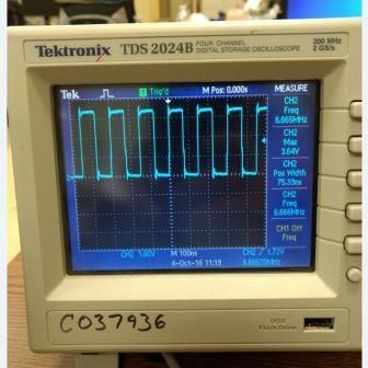
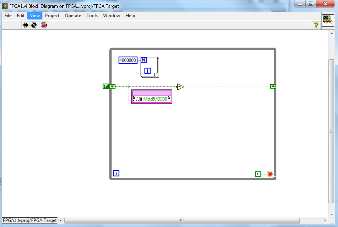
FPGA CRio do not give good digital outputs
I'm working on a project with the compact RIO fpga. I tried following the youtube tutorials and written tutorial, but I get no similar results in scanning FPGA interface.
I have attached my project. Here's the signal that I get from the Basic VI, which is a digital IO defined as output in a while loop. Alongside this, there is a loop for fundamentally changing the frequency of the digital signal from the top down. But whatever number I put in the loop for, it gives me the same frequency.
My thought process goes like this: If the CRio has a processing time of 40 MHz to a loop that cycles 400 times should give me a swing of 100 kHz output, which is not any number, I put in.
Any help is appreciated.
Thank you.
LabVIEW is almost certainly that compile to loop out like dead code (nothing happens so LabVIEW gets rid of it). I advise to use the loop timer function if you are looking to change the frequency or put everything in a timed loop. All in a timed loop will execute a tick.
-
sbRIO-9631 digital inputs/outputs using e/s node FPGAS and FPGA of i/o method node
Hello, I'm trying to configure my SBRio-9631 for the first time. I try to use the on boards to inputs and digital outputs. The following code will work? This is a simple "read the entries, 'or' some inputs and pass ' exits." I have to add "E/s method nodes FPGA" between my 'FPGA of i/o nodes"to get"modes of State of sorting for the input and output lines? Also, I can't simulate/test it works, by adding 5 VDC at the entrances, and not have any source of voltage output. Thank you for your time.
Hey, Spex,.
I really, really appreciate your help. Your follow up information was exceptional.
Thanks again for your help and your time.
gjmm
-
Hi all
We have NI 9421 digital input and digital output NI 9472 Modules. We can run these modules into a VI under the 9073 cRIO chassis. While we have added the FPGA target under the same chassis, we cannot use the modules. We also install the scan engine.
How can we use FPGAS and i/o Modules at the same time?
Once you add a target FPGA in CompactRIO chassis, when you deploy the code, the cRIO is configured for the FPGA mode, which requires a bitfile compiled to connect with the C Series modules. Remove the target FPGA or changing the mode of chassis in the project and by redeploying must reconfigure the cRIO for scan Mode, which allows you to use the IO module directly from the RT VI.
For more information, see this post.
-
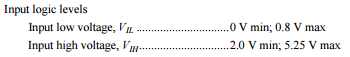
Digital FPGA of entry of the negative voltage
What is the maximum negative tension that the digital input on the FPGA can take without damaging it? I tried to look in the data sheet for the sRio 9636 and I can't.
Thank you
Hi, Berthe.
The sbRIO-9636 was DIO only on the OID (J502) and connectors MIO (J503). It's a bit different from the other variants sbRIO-96xx that others may have a RMC connector that has additional DIO.
Connectors IDC 50 pin DIO and MIO are 3.3V pins, but they are 5V tolerant inputs we have protection on the IDC DIO connector. VIL values and HIV are specified in the data sheet:
http://www.NI.com/PDF/manuals/373378d.PDF
These are the recommended conditions of use. If you need to know the maximum negative voltage to determine if your landing short of the runway is acceptable, this number to an absolute minimum is - 500 mV. I would recommend you choose the appropriate to your driver series termination resistors to minimize landing short of the runway, however. The absolute minimum even applies to the 3.3V RMC DIO as well.
-
Entered digital high frequency to the FPGA could not be detected OK
Hello
We want to connect the CMOS camera with PCIe-7842R with SCB68 box to analyze the image in the FPGA. There are PCLK (pixel clock) signal (36 MHz) and 8 bits of data.
On the 1st, we write a test program to ensure that we can detect the PCLK correct which is attached as program.png. The program is very simple there is a loop timed with 80 MHz, which should be enough take 36 MHz signal. If the value of 8000 "Digital 2", we should have 3600 (+ -1) like "digital." The reason why we (+ -1) is that we have no synchronization, is supported in this test program. And we can get the right result in this configuration.
2nd part, connect us data to 8-bit on FPGA and we get a wrong result of PCLK. Even connect us only 1 bit (which is labeled as DIO1 program) data, the PCLK is disturbed, and we can't find out why. The configuration of the connector is attached as connector.jpg.
We tried to make 2 very distant digital signals, but are still not. We tried to change the cables connected between SCB68 and FPGA of SHC68-68-RDIO cable for SHC68-68-RMIO cable because we think she may have better armor. We have a better result but still bad.
Now, we put "Digital 2" 8000 and we have about 3400 ~ 3500 as 'digital."which is false.
Does anyone have advice or commands on this problem? I'm very appreciate your kind help.
Thank you.
-
NEITHER 9205 fpga digital output
Hey Gang,
Hardware people left me with having to toggle the output of the NI 9205 DO0. I looked hard, but have not found anywhere where the PFIO and/or DO0 pin code feature is described. Part I/O of the application is written using the mode of FPGA. Of course, I would be able to control this bit of LabVIEW.
All responses will be welcome!
Thank you
Roger
Good,
I'm embarrassed!
I had inputs and outputs bass-ackward in my head. I took a digital Voltmeter to pin.
Everything is fine, except, perhaps, my brain!
Roger
-
PCIe-7842R (series R FPGA) digital output does not work properly
Greetings,
I'm having some problem show TTL the correct voltage with my PCIe-7842R FPGA board.
The block diagram of my code FPGA LV Moose appears in "analog - digital .png '. The idea was to convert an analog input (decimal value) to a binary code and 16-bit output by 16 DIO ports. I use the connection block SCB-68 has as the terminal and trendy on the FPGA 1 connector RDIO with SHC68-68-RDIO shielded cable.
The compiled code ok. But during the test, I noticed that some ports has no output TTL levels correctly. For example, for input 1000 decimal, I would expect binary code 0000001111101000. However, some ports (DIO #6, #7, #9, etc.), which are supposed to ~3.3V (1 digital) high TTL output, output actually 0.8V. I have attached the result measured in 'exit digital test.png '.
To ensure that the question was not because of the code of the LV, I did some more tests on DIO #6 with a simple example (simple digital output.png). The output was ~ 1V this time at the digital 1.
It's really confusing because of the digital Edition is supposed to be simple. I used the same FPGA card for controlling roller shutters with TTL signals before and it worked fine.
Does anyone have similar problems? Any suggestions are greatly appreciated.
iron_curtain wrote:
DIOs are connected to a controller digital galvo Cambridge Tech. But I measured the voltage at the terminals of the connector block.
If you unplug the controller galvo DIOs, do they look good (have the right voltages). Do you know how many of these entries to the need for controller? I think you hit the limit the total current available for EID within the Council.
-
Laser digital lock with Labview FPGA?
Hello
Sorry to bother if you are not interested in this issue of digital signal processing. We are looking for a possible digital solutions to our problem locked frequency cavity closed-loop laser (see attached PDF file for more details). The goal is to flatten the PZTs transfer function (cancel the resonances and anti-resonances and their phase shift matching) in the frequency domain, in addition to the normal PID control. Input/output necessary voltage signals are small (we have our own amplifiers high power for the PZTs), and their bandwidth must be at least of 50 kHz (100 kHz would be optimal).
Among various OR hardware/software (DSP, FPGA, cRIO etc.), would anyone recommend a cost-effective solution for rapid prototyping?
Thank you!
I would like to look at the FPGA PXI cards nor 7854r. I rate of 750 kHz, 1 MHz AO. According to the involved treatment, you might expect between 200 and 750 kHz closed control loop. If the treatment is very intense, it's probably something less than 200 kHz.
That said, the key to these performance levels is not trivial and great care and attention to detail must be used in the coding of the FPGA.
Good luck
Maybe you are looking for
-
Why do not upgrade Add-ons to work on the latest version of Firefox?
Have all these add-ons does not make much sense if you get a "not compatible with the latest version of Firefox. Of course, I bought an s4 to run the older versions. Firefox seems to have the mentality google alittle on themselves. Without the Add -
-
Always enter the ends of text - but I want the crossings of line!
Hello everyone. I was on the lookout here the half year past - as long as I've been programming in Labview, and now it's time to make my first post. The problem is a minor (but boring!) and probably a quick fix: I'm unable to add line breaks in text
-
Hallo! Lately, I've updated my LabView 8.6 to 8.6.1 then lately, I get the following error message when you use the VI atteched: Error-1073807338 at VISA near sornsg Close.vi-> output - Dima old.vi-> lambda_sornsg.vi-> COG.vi-> Ch2_main_with_s11.vi P
-
How does a Max flow to the network switch?
Want to total maximum flow of report on all ports of the switch 24 for a period of time. Able to obtain reports for individual interfaces. Thanks for any idea. Don Jarmon
-
Been happening since last night. Was working fine all day.